Conducted Emission Test and Improvement on SEPIC Topology Charger (CISPR 11)
- CircuitCopper

- Apr 4
- 4 min read
Updated: Apr 9
A recurring observation during EMC validation is straightforward: if conducted emissions fail, radiated emissions will also fail in most cases. The root cause is identical — excessive high-frequency current loops and poor control of switching node parasitic.
This case focuses on a SEPIC-based charger that failed conducted emission limits per CISPR 11.

1. Hot Loop Analysis of the DC/DC Stage
The dominant emission source in a SEPIC converter is the high di/dt switching loop. Improper layout directly increases differential-mode noise and field radiation.
a) Excessive distance between L1 and L2
In SEPIC topology, the energy transfer path between the two inductors must be tightly controlled. Large spacing increases loop area and parasitic inductance, which leads to:
higher voltage overshoot on the switching node
stronger magnetic field radiation

b) L1 and L2 Inductors are not magnetically coupled
Using two independent inductors instead of a coupled inductor structure increases ripple current and loop area. A coupled inductor:
reduces circulating current
minimizes differential-mode noise

c) No magnetic shielding
Unshielded inductors radiate magnetic fields directly into surrounding copper and air. This contributes to both:
near-field coupling into PCB traces
far-field radiated emissions
d) Input and output capacitors placed far apart
The high-frequency current loop in SEPIC includes:
input capacitor
switching device
inductors
coupling capacitor
If input/output capacitors are physically separated:
loop area increases
current return path becomes undefined
conducted noise increases significantly
2. Ground Plane Integrity Under Hot Loop
It is unclear whether a continuous solid ground plane exists under the switching loop.
This is critical.
Without a solid ground reference:
return current spreads unpredictably
loop inductance increases
EMI rises sharply
Best practice:
uninterrupted GND plane directly under switching components
no splits or voids under the hot loop
3. Absence of Input EMI Filter
The device does not include an input filter stage.
These guarantees conducted emission failure.
Minimum required structure:
differential-mode filter (LC or π filter)
high-frequency ceramic capacitors close to input
proper damping (avoid resonance amplification)
Without this:
switching noise is injected directly into supply lines
LISN measurement will exceed CISPR limits
4. Excessive Switching Node Copper Area
The switching node is routed as a wide copper area (large square shape).
This is a critical layout mistake.
Effects:
large dv/dt area acts as an antenna
strong capacitive coupling to nearby structures
increased radiated and conducted emissions
Correct approach:
minimize switching node copper area
keep it as small and compact as possible
avoid large pours or polygons

Summary (Root Causes)
The failure is not due to a single issue but a combination of layout and topology mistakes:
oversized high-current switching loops
lack of magnetic and electrical containment
missing input filtering stage
uncontrolled switching node geometry
Until these are corrected, both conducted and radiated emissions will remain out of compliance.
Test Setup and Power Supply Noise Filtering
Setup, and PS noise
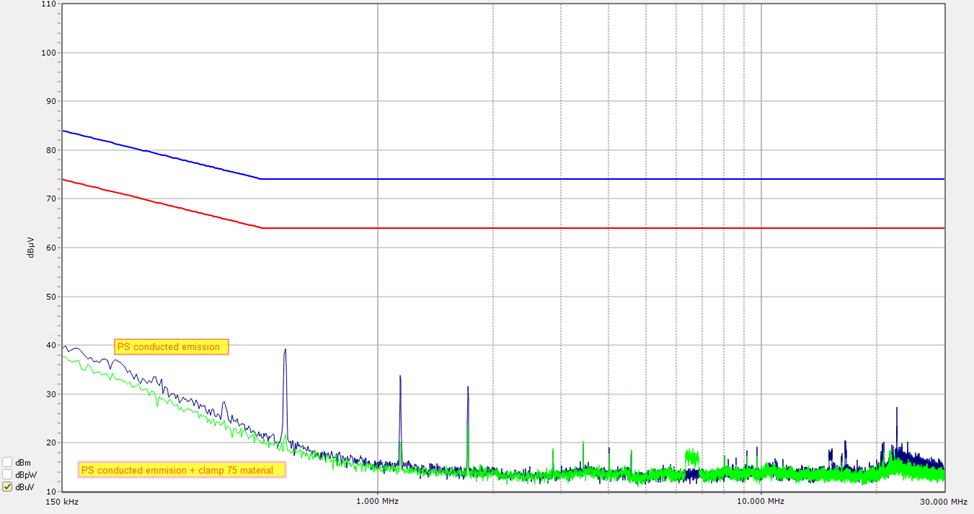

Device Setup and Measurements
First approach.

Second approach: four 22 µF, 50 V capacitors were installed at the input connector across the supply rails (positive to negative).

A slight reduction in emission peaks was observed, but the improvement was not significant.

Varying the input capacitance did not result in significant improvement. This indicates that the dominant noise is not effectively suppressed by capacitive filtering alone and requires a dedicated input filter.
Both common-mode choke (CMC) and LC filter approaches were evaluated. Based on standard EMI behavior, LC filtering targets differential-mode noise, while CMC is intended for common-mode noise.
Next step: a common-mode choke (CMC) was added at the device input, together with two 47 µF capacitors and an additional 2000 µF bulk capacitor. The results are shown below.

CMC Test 1: Partial Attenuation is observed with the common-mode choke; however, the reduction is not sufficient to meet the limits.

CMC Test 2: the emissions are significantly reduced and appear to meet the limits; however, the solution is not practical due to the large size of the common-mode choke and the use of bulky capacitors.

LC filter evaluation: A compact LC filter offers a practical and effective solution. It enables pre-compliance rework with minimal impact on the existing PCB layout, avoiding the need for a full redesign.

Results After LC Filter Implementation.

Conclusion
The implemented solution should be considered a mitigation rather than a complete fix. While the LC filter effectively reduces conducted emissions to acceptable levels, it does not eliminate the root causes of the noise.
To fully suppress or significantly reduce the emission sources, a redesign of the device is required, with primary focus on PCB layout optimization—particularly minimization of the high-current switching loops, proper component placement, and controlled switching node geometry.


Comments